Quattrone Nanofabrication Equipment / Instrumentation
ADT 7100 Dicing Saw
TOOL ID: BE-04
Workhorse dicing saw with precision dicing and alignment system. This is an automated tool with a 2″, DC-brushless, 1.2 kW, Front-mounted, Air-bearing Spindle (60 krpm Max.), with closed-loop turntable, and is optimized for multi-angle dicing of thin, tight tolerance products up to 200 mm x 200 mm.Go to Page
EVG 510 Wafer Bonder
TOOL ID: BE-01
The EVG501 Wafer Bonding System is a highly flexible R&D system that can handle small substrate pieces up to 100 mm wafers. The new tool supports a variety of bonding processes, such as anodic, glass frit, eutectic, diffusion, fusion, solder, and adhesive bonds, as well as other thermal processes, including oxide removal and high temperature bakes under a controlled atmosphere. The system also offers quick re-tooling with a conversion time of less than five
minutes, making it ideal for universities and R&D as well as small-volume production applications.
Features
- R&D and pilot line production
- Bonds up to 10 kN force at temperatures up to 450°C
- Real and low-force wafer wedge compensation system for highest yield
- Large process window: temperature uniformity <+/- 1% and pressure uniformity
<+/- 5%Go to Page
EVG 620 Wafer Bond Aligner
TOOL ID: BE-02
Known for its high level of automation and reliability, the EVG620 Bond Alignment System is designed for wafer-to-wafer alignment up to 150 mm wafer sizes. The EV Group´s bond alignment systems offer highest precision, flexibility, ease of use and modular upgrade capability and have been qualified in numerous high throughput production environments. The precision of EVG´s bond alignment system accommodates most demanding alignment processes in MEMS production and in emerging fields like 3D integration applications.
Features
- Supports bond alignment of double or triple wafer stacks up to 150 mm wafer sizes
- Manual or motorized alignment stage
- Fully motorized high resolution bottom side microscopes
- Windows® based user interface
- Quick tool change between different wafer sizes and different bonding applications
Kulicke & Soffa 4523 Wire Bonder
TOOL ID: BE-03
Aluminum wire wedge bonder. It provides digital controls with semiautomatic bonding cycle, but manual alignment.
The bonder can be operated in auto cycle or manual mode. The auto cycle mode is the preferred mode for most applications. Stitch bonding can be performed in the auto cycle mode. The manual mode is useful when the elevation between subsequent bond-pairs is substantially different.Go to Page
Cambridge NanoTech S200 ALD
TOOL ID: ALD-01
Savannah is equipped with high-speed pneumatic pulse valves to enable our unique Exposure Mode™ for thin film deposition on Ultra High Aspect Ratio substrates. This proven precision thin film coating methodology can be used to deposit conformal, uniform films on substrates with aspect ratios of greater than > 2000:1.
The Penn Savannah is capable of holding substrates of different sizes (up to 200mm). It is equipped with six precursor lines for deposition of Al2O3, HfO2, TiO2, and SiO2.Go to Page
Denton Vacuum Explorer 14 Sputterer
TOOL ID: PVD-05
- Open load system in sputter-down configuration
- Two DC guns
- Able to co-sputter one DC and one RF source
- One RF gun
- Cryo pumped with automated interface
- Automated control of film thickness
- Pieces through 150mm wafers
- Wafer platen rotation with cooling
- Substrate cleaning
Evatec Clusterline 200 II Sputter
TOOL ID: PVD-06
The system is owned and managed by the Olsson Group at UPenn. Inquiries into using the system should be made to staff via an email at qnf-process@lists.seas.upenn.edu .
The tool is configured to sputterer piezo-electric materials, including Al and Sc.Go to Page
Plasma enhanced chemical vapor deposition systemGo to Page
Kurt J. Lesker PVD 75 – E-Beam/Thermal Evaporator
TOOL ID: PVD-02
- Two thermal sources
- Four pocket e-beam at 10kV
- Cryo pumped with automated interface
- Automated control of film thickness
- Pieces through 150mm wafers
- Wafer platen rotation with cooling stage
Kurt J. Lesker Nano 36 Thermal Evaporator
TOOL ID: PVD-01
- Four thermal sources
- Quick turbo pumping automated interface
- Automated control of film thickness
- Pieces through 150mm wafers
- Wafer platen rotation
Kurt J. Lesker PVD 75 PRO-Line E-Beam Evaporator
TOOL ID: PVD-04
- Load locked system
- Four pocket e-beam at 10kV
- Cryo pumped with automated interface
- Automated control of film thickness
- Pieces through 150mm wafers
- Wafer platen rotation
Kurt J. Lesker PVD 75 PRO-Line Sputterer
TOOL ID: PVD-03
- Load locked system
- Three DC guns
- Able to co-sputter two DC sources
- One RF gun
- Cryo pumped with automated interface
- Automated control of film thickness
- Pieces through 150mm wafers
- Wafer platen rotation with heating
Sandvik LPCVD & Anneal Furnace
TOOL ID: CVD-02
The Sandvik LPCVD consists of 4 horizontal tubes:
Tube 1: Wet/Dry Silicon Oxide deposition.
Tube 2: Low Stress Silicon Nitride deposition.
Tube 3: Clean anneal.
Tube 4: General anneal.
The tool is configured for 100 mm (4″ wafers) and can process up to 50 wafers at a time.
Go to Page
Molecular Vapor Deposition SystemGo to Page
Oxford Instruments Plasma Lab 100 PECVD
TOOL ID: CVD-01
This is a load locked PECVD system capable of depositing SiO2, Si3N4 and a-Si. Process temperatures range from room temperature through 400C. In addition to standard RF plasma, there is a low frequency source for stress tuning films. The system handles 4”/100mm wafers.Go to Page
SCS Labcoter 2 (PDS 2010) Parylene Deposition System
TOOL ID: PVD-07
The SCS Labcoter 2 (PDS 2010) vacuum deposition system is specifically designed to bring Parylene technology to the laboratory. Its size and portability make it the ideal choice for universities and research institutions looking to to develop and design with Parylene conformal coatings.
As a high quality, compact coating unit, the PDS 2010 is well suited for a range of applications, including circuit boards, sensors, wafers, medical devices and elastomeric components for research, development and repair.Go to Page
SMI MOCVD
TOOL ID: CVD-04
The system is owned and managed by the Jariwala Group at UPenn. Inquiries into using the system should be made to staff via an email at qnf-process@lists.seas.upenn.edu .
The systems is a Metal-organic chemical vapor deposition system configured with the following precursors: (CH3)2Se, Mo(CO)6, (CH)3 In, H2, H2S.Go to Page
Tousimis 931-C Critical Point Dryer
TOOL ID: CPD-01
- Enables drying of delicate samples through the use of liquid carbon dioxide as a transitional fluid which has zero surface tension at the critical point (1072 psi at 31 C)
- Can process pieces up to several 100 mm substrates
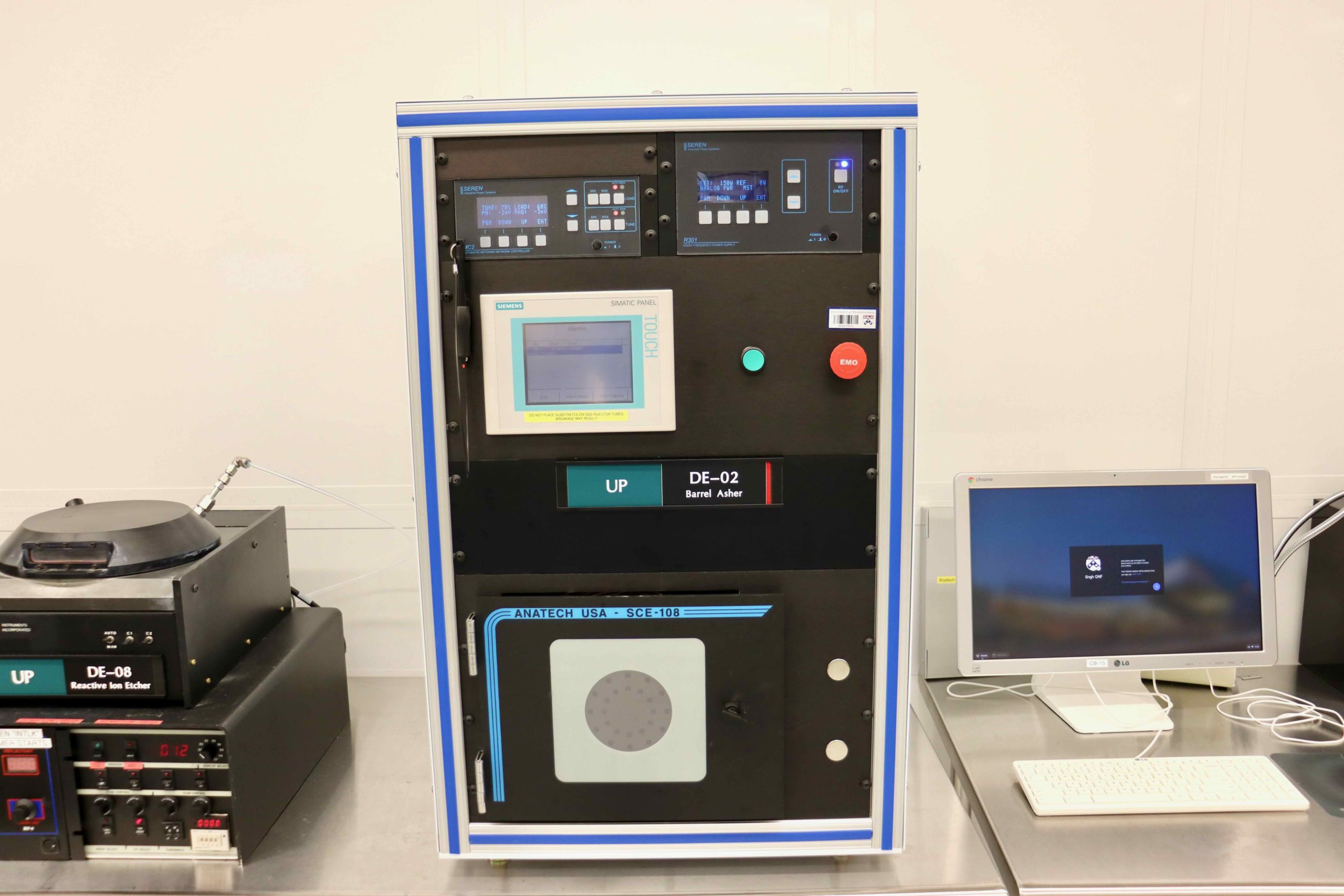
Anatech SCE 106 Barrel Asher
TOOL ID: DE-07
Anatech USA’s SCE-100 Series Inductively Coupled (ICP) Plasma systems are extremely effective for a Plasma Ashing process to remove organics prior to thin film deposition and/or chemical analysis of remaining inorganics.
Process gases are CF4, O2, Ar and N2. Sample sizes are pieces to 150mm round wafers.Go to Page
Downstream RIEGo to Page
Oxford Instruments Plasma Lab 80+ RIE
TOOL ID: DE-04
A compact open-loading tool for Reactive Ion Etching – Oxford 80+ RIE
The Oxford 80+ offers versatile reactive ion etch solutions on one platform with convenient open loading. This compact, small footprint system is easy to use, with no compromise on process quality.
It is ideally suited to R&D or small-scale production, and can process from the smallest wafer pieces to 200mm wafers. The open load design allows fast wafer loading and unloading, ideal for research, prototyping and low-volume production.
- 600W RF generator
- Up to 200mm wafers
- Process gases: CF4, Ar, O2, SF6 and CHF3
- Excellent etch control
- Excellent process control
- Documented baseline recipes are provided by Penn’s QNF staff
Oxford PlasmaPro 100 Cobra ICP
TOOL ID: DE-5
The PlasmaPro 100 Cobra ICP RIE system utilizes a high-density inductively coupled plasma to achieve fast etch rates. The process modules offer excellent uniformity, high-throughput, high-precision and low-damage processes for wafer sizes up to 4″ or 100mm.
The tool is connected to the following gases: BCl3, Cl2, Ar, O2, SF6, CF4, and CHF3.
SPTS Rapier Si DRIE
TOOL ID: DE-03
With an installed base of over 1000 DRIE process modules, SPTS’ market-leading position is spearheaded by the Rapier module, which etches Si using Bosch switched processing as well as non-switched etching for tapered profiles, wafer thinning and via reveal.
Advantages of SPTS Si DRIE
- Patented dual plasma source design with independently controlled primary and secondary decoupled plasma zones, with independent dual gas inlets. This results in a highly concentrated and uniformed distribution of radicals.
- High etch rate
- Excellent uniformity
- Controls tilting of deep features across the wafer
- Inherent multi-mode flexibility also allows complementary oxide etching within the same hardware.
Delivering unparalleled process capability with world-class productivity & cost of ownership benefits, SPTS’ DRIE process modules are used in a wide variety of applications across multiple end markets.Go to Page
RIE, Multipurpose IIGo to Page
RIE, Multipurpose IIIGo to Page
Xactix e1 XeF2 Etch System
TOOL ID: DE-6
Isotropic etching of silicon using xenon difluoride is an ideal solution for releasing MEMS devices. XeF2 shows high selectivity to silicon over almost all standard semiconductor materials including photoresist, silicon dioxide, silicon nitride and aluminum. Being a vapor phase etchant, XeF2 avoids many of the problems typically associated with wet or plasma etch processes.
Built for simplicity, and a small footprint, the Xactix® e1TM is the ideal solution for requiring an R&D xenon difluoride etching system. This table top etcher is ideal for small volumes in QNF.
Key Benefits
- Simple & reliable
- Great for working with small samples and wafers
Agilent E3620
- Output 1: 0 to 25 V, 0 to 1 A
- Output 2: 0 to 25 V, 0 to 1 A
- Power (max): 50 W
- Ripple & Noise from 20 Hz to 20 MHz
- Normal Mode Voltage rms: 350 µV
- Peak-to-Peak: 1.5 mV
- Load & Line Regulation
- 01% + 2mV
- Meter Resolution
- Voltage: 10 mV (0-20 V), 100 mV, (>20 V)
- Current: 1 mA
Micromanipulator 4060 Probe Station
TOOL ID: MET-09
The Micromanipulator Model 4060 probe station is a high efficiency general purpose 6 – 8” (150 – 200mm) manual analytical probe station. The 4060 is designed for ease of use in everyday failure analysis, device characterization, and reliability testing applications. The 4060 station combines the value of efficient use with the confidence of consistent, accurate electrical and mechanical performance. The system is configured with two Keithley 2450 Graphical SourceMeter (SMU) Instruments.
Keithley 2400
Keithley’s Series 2400 Source Measure Unit (SMU) Instruments are designed specifically for test applications that demand tightly coupled sourcing and measurement. The SourceMeter provides precision voltage and current sourcing as well as measurement capabilities. Each SourceMeter SMU instrument is both a highly stable DC power source and a true instrument-grade 6½-digit multimeter. The power source characteristics include low noise, precision, and readback. The multimeter capabilities include high repeatability and low noise. The result is a compact, single-channel, DC parametric tester. In operation, these instruments can act as a voltage source, a current source, a voltage meter, a current meter, and an ohmmeter.Go to Page
Jandel Multi Height Four Point Probe
TOOL ID: MET-08
- Allows probing of wafers, ingots, or samples of widely varying dimensions
- Locking mechanism allows the arm to be moved up and down the steel pole and locked to suit any sample height
- Plug attached to the arm prevents the wiring from getting entangled with samples, fingers etc
- Smooth base for positioning samples
- Includes one Jandel Cylindrical probe head
Optical Inspection Scope #1
- 5x, 10x, 20x, 50x and 100x objectives
- Bright field and dark field
- Nomarski imaging
- Digital frame grabbing and measurement software
Optical Inspection Scope #2
- 5x, 10x, 20x, 50x and 100x objectives
- Bright field and dark field
- Nomarski imaging
- Digital frame grabbing and measurement software
Optical Inspection Scope #3
- 5x, 10x, 20x, 50x and 100x objectives
- Bright field and dark field
- Nomarski imaging
- Digital frame grabbing and measurement software
Zeiss Axio Imager M2m Microscope – 1
TOOL ID: MET-12
In Normal operation, it is possible to observe ~2 µm diameter objects in the reflected and transmitted mode. Furthermore, the following contrasting techniques are available: bright-field, dark-field, Circular Differential Interference Contrast (C-DIC) using circularly polarized light, polarization contrast, and polarization with additional retarder. The image snapped can be analyzed using the annotation tool on
the software.
In Extended Focus operation, the images of 3D structure can be acquired at different focus positions, and automatically combined as a sharp 2D image.
In Panorama operation, the images acquired can be stitched, so that the optical microscope image of the wide object can be obtained.Go to Page
IPG Photonics IX280-DXF Laser System
TOOL ID: LMM-02
The IX280-DXF is a highly flexible laser micro-machining system for multipurpose, R&D and production applications. The system combines a Class 1 workstation integrated with a fiber laser and all necessary software.
Cutting Applications
- Ceramics, Metals, Polymers and Semiconductor Materials
- Patterning of ITO and other Thin-films
Drilling Applications
- Hole Diameters down to 15 μm
Class 1 Micromachining Workstation
- Lasers at 532 or 1064 nm
- Pulse Energy up to 15 Joules (1064 nm)
- X-Y Positional Accuracy: <3 μm
- Z-theta Accuracy: <10 μm, ±0.02°
- Galvanometer Scanner or Fixed Optics
- Thermal Cutting Head
- Step and Scan Stage/ Galvo Integration
Vision System Resolution 0.12 μm/ pixel
DXF and CSV File Interface
IPG Microsystems’ IX-255
TOOL ID: LMM-01
The IPG IX-255 Excimer Laser is a highly flexible UV laser micromachining system for multi-purpose, R&D and production applications. The system combines a Class 1 workstation integrated with a proprietary UV (193nm) laser and beam shape selector (infinitely variable rectangular and discrete circular) to machine transparent samples such as plastic, glass, and PDMS.
Applications
- Micro Drilling
- Annealing
- Thin-film Removal
- Laser Lift-off (LLO)
- Dicing
Features
- Pre-set Configurations for High Fluence and Large Field of View Applications
- Selectable Beam Shapes for Automated, Complex Micromachining
- Precision Stages with <3 μm Motion Control Accuracy
- Dual Magnification Vision System with Sub-micron Part Alignment
- 193 nm Laser
- Linear Mask Changer for Complex Features and Shapes
Mask alignerGo to Page
Negative Resist Hot Plate Tower
Each hot plate tower in QNF is outfitted with (6) Torrey Pines digital thermal hot plates that can be heated to 350C with controlled ramping. In addition, there is a stainless steel gravity convection capable of heating to 300C in each tower as well.Go to Page
Positive Resist Hot Plate Tower
Each hot plate tower in QNF is outfitted with (6) Torrey Pines digital thermal hot plates that can be heated to 350C with controlled ramping. In addition, there is a stainless steel gravity convection capable of heating to 300C in each tower as well.Go to Page
Soft Lithography Hot Plate Tower
Each hot plate tower in QNF is outfitted with (6) Torrey Pines digital thermal hot plates that can be heated to 350C with controlled ramping. In addition, there is a stainless steel gravity convection capable of heating to 300C in each tower as well.Go to Page
Beamer and Tracer Lithography Software
TOOL ID: EBL-02
The Quattrone Nanofabrication Facility (QNF) features state-of-the-art software for next-generation electron beam (e-beam), mask aligner and laser lithography. Specifically, the software package, BEAMER and TRACER, offers advanced data preparation, 2D and 3D proximity effect correction (PEC), process modeling and simulation for direct write applications in e-beam and laser lithography.Go to Page
Elionix ELS-7500EX EBL
TOOL ID: EBL-01
Ultra-high precision lithography with a resolution of 10 nm and with high stitching and overlay accuracy.
Specifications
Electron gun emitter | ZrO/W thermal field emitter |
Acceleration voltage | 50kV,30kV,20kV |
Minimum line width | 10nm |
Specimen size | 6″ (maximum) |
Features
Ultra-fine lithography.
- The 2-nm diameter spot beam allows the ultra fine pattern writing of 10 nm width. ELS-7500EX incorporates SEM function that serves for exposed pattern observation.
High stitching and overlay accuracy.
- ELS-7500EX provides overlay accuracy of 30 nm that supports mix-and-match with photolithography.
- The recipe function, with saved optimum beam settings, provides the ease of the operation.
- The stage with a built-in laser interferometer and beam positioning resolution of 0.31 nm with an 18-bit DAC provide a stitching accuracy of 30 nm.
High performance with compact configuration. Ease of operation with PC control.
- Integration of a Windows compatible GUI and CAD realizes a small footprint.
- Electron optical condition control and CAD pattern design can be accomplished by simply using a mouse. A very user friendly system.
Application gallery
R = 100μm blazed circle
(Pitch in the radius direction 1.0μm)
L&S: 80 nm
Resist Thickness: 1.5μm || Line width: 25 nmGo to Page
Genesis HMDS Vapor Prime Oven
TOOL ID: OVN-01
While wet chemical surface modification can be done, vapor phase deposition has become the preferred method for coating surface as the process environment can be tightly controlled. Due to liquid surface tension, the wet process can have poor contact between the solution and the surface, especially when the surface is textured with small features. Another problem with wet processing, or solution phase deposition, is this process typically uses water.
Standard recipes include HMDS priming and image reversal with ammonia chemistry. Other chemistry and related SAM coatings can be developed on request.Go to Page
Heidelberg DWL 66+Laser Writer
Nanonex 2600 Nanoimprinter and Mask Aligner
The Nanonex NX-2600 is a full wafer nanoimprinter and photolithography aligner. It is capable of all imprint forms: thermal, photo-curable, embossing and photolithography, with sub-5nm imprinting resolution and sub-1 micrometer alignment accuracy. Based on the Nanonex unique patented Air Cushion PressTM technology, the NX-2600 offers unsurpassed uniformity regardless of backside topology, wafer or mask flatness, or backside contamination. This ACP technology also eliminates lateral shifting between the mask and substrate, which significantly increases mask lifetime.
Standard nanoimprint resists are provided. Front and backside mask alignment.Go to Page
Nanoscribe Photonic Professioal GT
TOOL ID: LW-02
The NanoScribe Photonic Professional GT, a nano-micro 3D laser printer for a variety of research applications. The tool has been demonstrated to enhance life science research in the areas of cell/extracellular matrix interaction, targeted drug delivery, cell migration, tissue engineering and 3D cell culture. The tool’s ease of use shortens the learning curve and will enable a new era of research for our users. Using two photon polymerization, the tool is capable of writing using the ultra-precise piezo stage or high speed galvanometer. Go to Page
Ovens and Hotplate Towers
Each hot plate tower in QNF is outfitted with digital thermal hot plates that can be heated to 350C with controlled ramping. In addition, there are stainless steel gravity convection ovens capable of heating to 300C in each tower as well. Several baking stations are located throughout the QNF, each dedicated to specific resist process and polymer curing.Go to Page
The Raith EBPG5200+ is an electron beam lithography tool capable of high-resolution patterning at 100 kV. It has a 125 MHz pattern generator, a maximum current of 350 nA, and a 1 mm mainfield size. It has an automatic aperture changer, automatic and dynamic focus and stigmation, and automatic alignment. The EBPG can achieve linewidths <8nm with stitching and overlay accuracy better than 10nm.
Applications
- Large-scale, high-speed patterning of positive and negative e-beam resists with features from <10 nm to micron/mm scale
Allowed Materials
- Standard semiconductor materials
- Low vapor pressure metals
- Resists
Resist and Polymer Spinners
The QNF maintains several resist and polymer spinners throughout the cleanroom. Each spinner is dedicated to specific resist and polymer types to reduce cross contamination.
- Maximum speed of 10,000 rpm
- User friendly programmable interface
- Programmable step functions (up to 10 steps per recipe)
- Programmable process control
- Wafer sizes from pieces through 150mm
Negative Resist Spinner
- Two Spinners
- Maximum speed of 10,000 rpm
- User friendly programmable interface
- Programmable step functions (up to 10 steps per recipe)
- Programmable process control
- Wafer sizes from pieces through
-300mm capable bowl sizesGo to Page
Positive Resist Spinner
- Three Spinners
- Maximum speed of 10,000 rpm
- User friendly programmable interface
- Programmable step functions (up to 10 steps per recipe)
- Programmable process control
- Wafer sizes from pieces through 150mm
SUSS MicroTec AS8 AltaSpray Coater
TOOL ID: RC-01
Automated Spray Coater for High Topographies
SUSS MicroTec’s proprietary AltaSpray coating technology is a unique resist deposition method that is capable of producing highly uniform resist films on different 3-D microstructures. The AltaSpray technology is capable of coating 90° corners, KOH etched cavities, Through Silicon Vias (TSVs) or lenses with topographies ranging from a few micron to 600µm or more. The ability to produce conformal resist coatings on severe topography makes them the ideal choice for R&D, MEMS, 3D-Integration and Wafer Level Packaging applications like 3D image sensor packaging.
Wafer sizes from pieces to 200mm. Common resists sprayed are SU-8, S1800 and various AZ formulations.
SUSS MicroTec MA-6 Mask Aligner
TOOL ID: MA-01
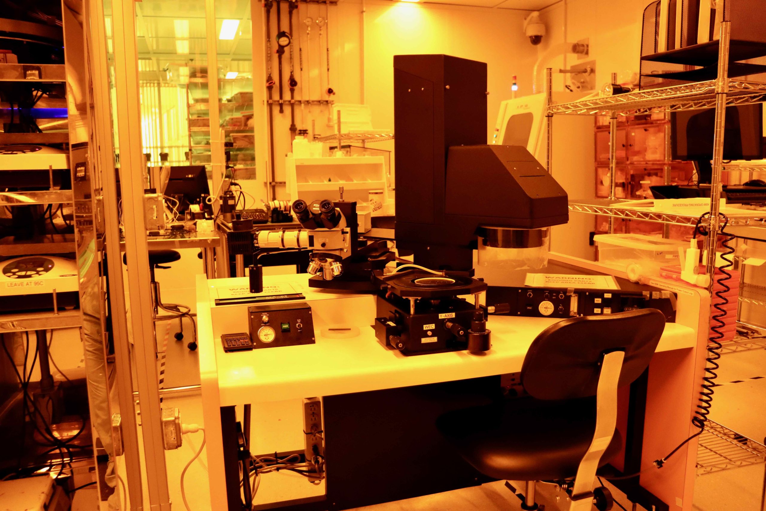
The Dedicated Solution for Industrial Research and Operator Assisted Alignment
Designed for R&D, pilot line and production environments, the MA/BA6 Gen3 enables production-friendly research. It allows easy and cost effective process transfer from laboratory to production. Key components such as high resolution optics, precise alignment system and graphical user interface perfectly match with the SUSS production aligner platform.
- High resolution (HR) optics allows patterning of structures below 0.5μm
- Operator assisted and auto alignment permits down to 0.25μm alignment accuracy
- Advanced automatic functions for maximum process control
- Process compatibility with automatic equipment
- Optimized split field microscope with direct viewing and/or LCD flat screen options
- Allows utilization of tool sets from the previous MA/BA6 platform
- Pieces through 150mm wafers.
Filmetrics F40 Reflectometer
TOOL ID: MET-04
The F40 has an integrated color video camera that allows exact monitoring of the film thickness measurement spot. Thickness and index can be measured in less than a second. The F40 product family is for applications that require a spot size as small as 1 micron.Go to Page
Filmetrics F50 Reflectometer – UV Filter
TOOL ID: MET-03
The Filmetrics F50 family of products can map film thickness as quickly as two points per second. A motorized R-Theta stage accepts standard and custom chucks for samples up to 200mm in diameter. This system has a UV filter installed and is used for measuring film thicknesses of UV sensitive photoresists. A second F50 system without UV filters is located in the QNF (MET-11).
Map patterns can be polar, rectangular, or linear, or you can create your own with no limit on the number of measurement points. Dozens of pre-defined map patterns are supplied.Go to Page
J.A. Woollam V VASE Spectroscopic Ellipsometer
TOOL ID: MET-06
The VASE is one of the most accurate and versatile ellipsometer for research on all types of materials: semiconductors, dielectrics, polymers, metals, multi-layers, and more.
It combines high accuracy and precision with a wide spectral range up to 300 to 1100nm. Variable wavelength and angle of incidence allow flexible measurement capabilities including:
- Reflection and Transmission Ellipsometry
- Generalized Ellipsometry
- Reflectance (R) intensity
- Transmittance (T) intensity
- Cross-polarized R/T
- Depolarization
- Scatterometry
- Mueller-matrix
KLA Tencor P7 2D Profilometer – 1
TOOL ID: MET-01
The P-7 stylus profiler offers industry leading measurement repeatability for reliable measurement performance. The surface measurement system has 150 mm scan length standard – the only stylus profiler on the market to offer long scan capability without the need for stitching. The UltraLite® sensor includes dynamic force control, excellent linearity, and the highest vertical resolution making it the best sensor available on a surface measurement system. Finally, this stylus profiler’s surface measurement system includes point-and-click operation and the productivity package to offer the easiest to use tool on the market with the features required by university, R&D, and production environments.
The P-7 Stylus profiler is capable of addressing a wide range of surface measurements and applications:
- Thin film step height measurements
- Thick film step height measurements
- Photo resist / soft films
- Etched trench depth
KLA Tencor P7 2D&3D/stress profilometer
TOOL ID: MET-02
The P-7 stylus profiler offers industry leading measurement repeatability for reliable measurement performance. The surface measurement system has 150 mm scan length standard – the only stylus profiler on the market to offer long scan capability without the need for stitching. The UltraLite® sensor includes dynamic force control, excellent linearity, and the highest vertical resolution making it the best sensor available on a surface measurement system. Finally, this stylus profiler’s surface measurement system includes point-and-click operation and the productivity package to offer the easiest to use tool on the market with the features required by university, R&D, and production environments.
The P-7 Stylus profiler is capable of addressing a wide range of surface measurements and applications:
- Thin film step height measurements
- Thick film step height measurements
- Photo resist / soft films
- Etched trench depth
- Materials characterization for surface roughness and waviness
- Surface curvature and form
- 2D stress of thin films
- Dimensional analysis and surface texture
- 3D imaging of various surfaces
- Flatness or curvature
- Defect review and defect analysis
Zygo NewView 7300 3D Surface Profiler
TOOL ID: MET-05
The NewView 7300 white light interferometer (profilometer) is a powerful tool for characterizing and quantifying surface roughness, step heights, critical dimensions, and other topographical features with excellent precision and accuracy. All measurements are nondestructive, fast, and require no sample preparation. Profile heights ranging from < 1 nm up to 20000 µm at high speeds, independent of surface texture, magnification, or feature height!
Using ZYGO’s Coherence Scanning Interferometry (CSI) technology, the NewView™ 7300 3D optical surface profiler easily measures a wide range of surfaces, including smooth, rough, flat, sloped, and stepped surfaces.
Key Features:
• Fast non-contact measurements
• Sub-angstrom Z resolution
• Leading-edge precision & gage capability
• Enhanced optical imagingGo to Page
IPG Microsystems IX-255
A highly configurable laser work cell for general purpose and small-scale production applications. The system combines a Class 1 workstation integrated with a fiber laser and all necessary software. Configurable options, available with initial order or as a field upgrade, include: Ablation or Thermal Cutting & Drilling, Part Handling & Moving, Beam Formation, Delivery & Scanning, Vision System and Alignment. Additional options and accessories further extend the versatility and application of this easy- to-use laser micromachining system. The IX-200-F can be configured with basic functionality as an entry-level system, as a fully equipped, highly precise machining tool compatible with any micromachining application, or anywhere in between. The modular design allows users to buy the capability needed today and expand through field upgrades as requirements evolve.
Cutting Applications
- Ceramics, Metals, Polymers and Semiconductor Materials
- Patterning of ITO and other Thin-films
Drilling Applications
- Hole Diameters down to 15 μm
Class 1 Micromachining Workstation
- Lasers at 532 or 1064 nm
- Pulse Energy up to 15 Joules (1064 nm)
- X-Y Positional Accuracy: <3 μm
- Z-theta Accuracy: <10 μm, ±0.02°
- Galvanometer Scanner or Fixed Optics
- Thermal Cutting Head
- Step and Scan Stage/ Galvo Integration
Vision System Resolution 0.12 μm/ pixel
DXF and CSV File Interface
IPG Microsystems’ IX-200F
A highly flexible UV laser micromachining system for multi-purpose, R&D and production applications. The system combines a Class 1 workstation integrated with a proprietary UV laser, tool shape selector and software for complex automation sequences.
Applications
- Micro Drilling
- Annealing
- Thin-film Removal
- Laser Lift-off (LLO)
- Dicing
Features
- Pre-set Configurations for High Fluence and Large Field of View Applications
- Selectable Beam Shapes for Automated, Complex Micromachining
- Precision Stages with <3 μm Motion Control Accuracy
- Dual Magnification Vision System with Sub-micron Part Alignment
- 193 nm Laser
- Linear Mask Changer for Complex Features and Shapes
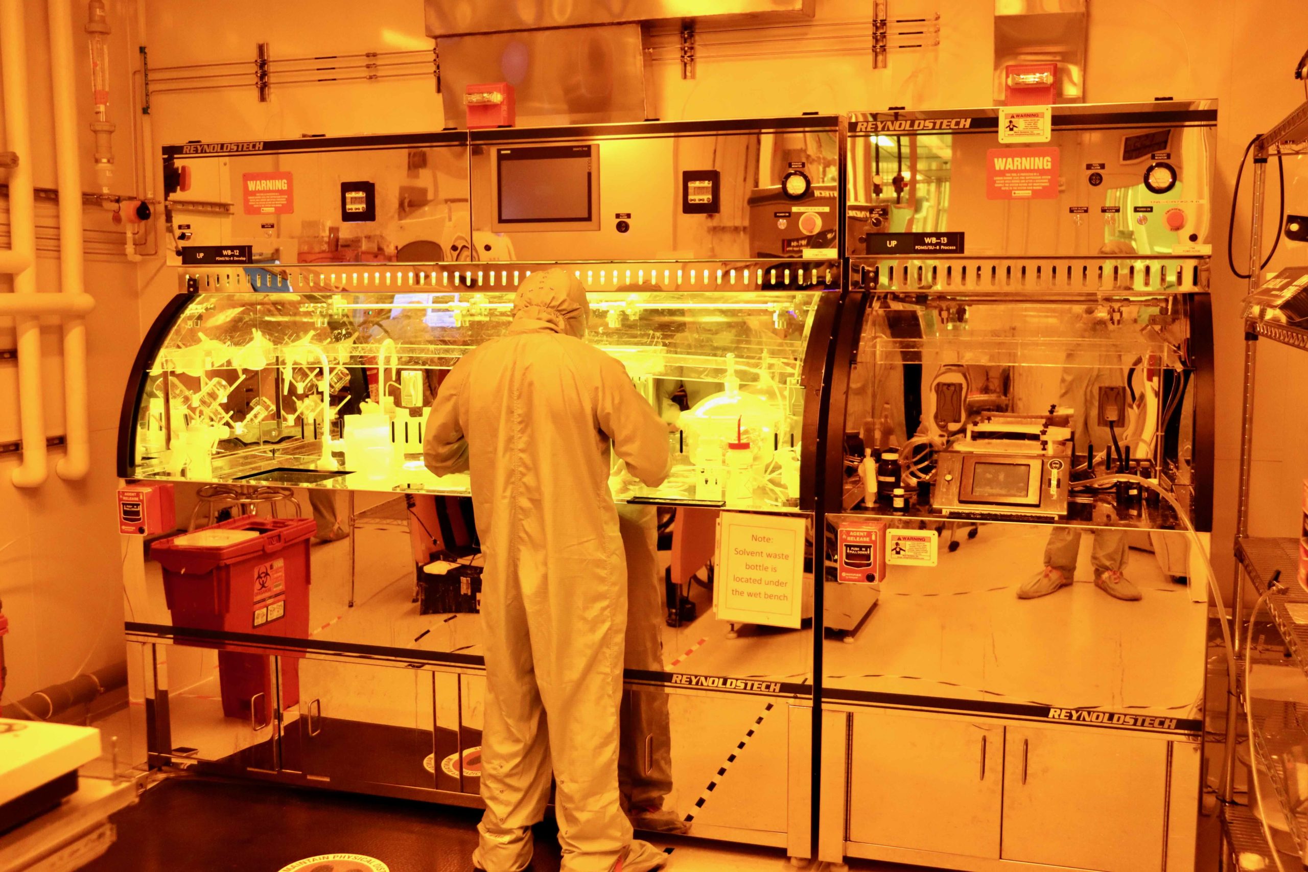
Reynolds Tech Positive Photoresist Spinner Bench
This is a laminar flow bench with three spinners with rotation speeds from 1-10,000 RPM. Wafer sizes from pieces to 150mm. Solvent drains and nitrogen guns at each spinner station.Go to Page
Reynolds Tech Positive Photoresist Develop Bench
This is a positive photoresist developing bench with integrated single wafer rinsing for samples up to 150mm. Typical developers are 0.26N TMAH based.Go to Page
Reynolds Tech Negative Photoresist Spinner Bench
This is a laminar flow bench with two spinners with rotation speeds from 1-10,000 RPM. Wafer sizes from pieces to 150mm. Solvent drains and nitrogen guns at each spinner station. PDMS can be spun in one of the spin station; the other station is typically used for SU-8, LOR and related negative resists.Go to Page
Reynolds Tech Negative Photoresist Develop Bench
This is a negative photoresist developing bench with integrated single wafer rinsing for samples up to 150mm. Typical developers PGMEA based for SU-8. Another application is use of resist strippers that can be disposed in the integrated solvent drains.Go to Page
Reynolds Tech E-Beam Resist Spin & Develop Bench
This is a laminar flow bench containing one spinner with rotation speeds from 1-10,000 RPM. Wafer sizes from pieces to 150mm. Solvent drains and nitrogen guns at each spinner station. This bench is also used for e-beam resist development. Standard PMMA and ZEP 520A are provided.Go to Page
HF Process Bench
- Substrates up to 150mm
- 5:1 BOE tank (room temperature)
- Cascade rinse tank
- Goose neck sink
- N2 and DI water guns
Electroplating Process Bench
- Substrates up to 150mm
- Two stations for plating Cu, Ni or Au
- Goose neck sink
- N2 and DI water guns
Solvent Process Bench
- Substrates up to 150mm
- Heated ultrasonic tank
- Goose neck sink
- N2 and DI water guns
Acid Process Bench
- Two process stations
- Substrates up to 150mm
- Cascade rinse tank
- Goose neck sink
- N2 and DI water guns
Acid Process Bench
- Substrates up to 150mm
- Heated ultrasonic tank
- Goose neck sink
- N2 and DI water guns
SU-8/PDMS Spin Bench
- Substrates up to 150mm
- Spinner for SU-8, PDMS and related soft materials
Automatic Bottle Washer
- Automatic bottle washer
- Capable of rinsing three bottles simultaneously
Leica Critical Point Dryer
TOOL ID: CPD-01
The critical point dryer can dry delicate samples without any damaging effect of surface tension, using the zero surface tension of carbon dioxide at the critical point at 31°C and 1072 psi (cf. the critical point of water = 374°C and 3212 psi).Go to Page
Verteq Superclean Spin Rinse Dryer
TOOL ID: SRD-01
The SuperClean 1600-3 is a single cassette, front-loading, programmable rinser/dryer used to rinse and dry round substrates that are 100mm or 150mm in diameter. The system rinses to a DI water resistivity of ~12 Mohm before the heated nitrogen drying cycle commences.Go to Page